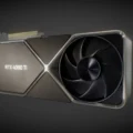
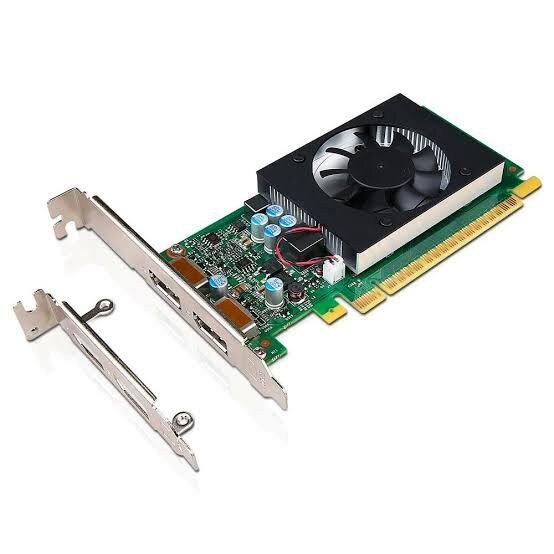
NVIDIA GeForce GT 730
The NVIDIA GeForce GT 730 specs bring 0.585 billion transistors featuring a DDR3 Memory type and a 1024MB memory size. This GPU was manufactured using TSMC 40nm process technology.
Specs And Benchmark
Board Design
| Available | Jun 2014 |
| Foundry | TSMC |
| Type | Desktop |
| Interface | PCIe 2.0 x16 |
| Generation | GeForce 700 |
| Outputs | 1x DVI, 1x HDMI 1.3a, 1x VGA |
| Power Connectors | None |
| TDP | 49W |
| Suggested PSU | 200W |
GPU Features
| DirectX | 12 (11_0) |
| OpenGL | 4.6 |
| OpenCL version | 1.1 |
| Vulkan version | N/A |
| Shader Model | 5.1 |
| CUDA | 2.1 |
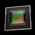
Graphics Processor
| Die Size | 116mm² |
| GPU Variant | GF108-400-A1 |
| GPU name | GF108 |
| Transistor count | 585 million |
| Architecture | Fermi |
| Process Node | 40 nm |
Clock Speeds
| Boost Clock | - |
| Base Clock | - |
| Memory Clock | 900MHz |
Memory Specs
| Memory Types |
DDR3 |
| Max Memory Size | 1024MB |
| Max Memory Bandwidth | 28.80 GB/s |
| Memory Bus | 128bit |
Render Config
| Shading units | 96 |
| L1 cache | 64 KB (per SM) |
| L2 cache | 256KB |
| TMUs | 16 |
| ROPs | 4 |
| GPU Major Cores | 2 |
Theoretical Performance
| FP32 (float) | 268.8 GFLOPS |
| FP64 (double) | 22.40 GFLOPS |
| Texture Rate | 11.20 GTexel/s |
| Pixel Rate | 2.800 GPixel/s |